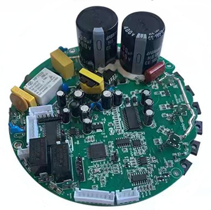
The Printed Circuit Board (PCB) is constructed using electrically linear materials, implying that its impedance should remain constant. However, the PCB introduces nonlinearity into the signal due to its spatial layout concerning the current flow path.
In a PCB design, when an amplifier draws current from a power supply, the current flows through a bypass capacitor and enters the load via the amplifier. It then returns to the ground plane from the ground terminal of the load or the shield of the PCB output connector, passes through another bypass capacitor, and returns to the original power source.

Contrary to the misconception that current flows through the path with minimum impedance, the amount of current flowing through various impedance paths is proportional to their conductivity. In a ground plane, multiple low-impedance paths often exist through which a significant proportion of ground current flows. Some of these paths are directly connected to the bypass capacitor, while others excite the input resistance before reaching the bypass capacitor.
The placement of bypass capacitors at different positions on the PCB causes the ground current to flow through different paths, leading to “spatial nonlinearity.” As a consequence, certain polarity components of the ground current may predominantly flow through the ground of the input circuit, causing distortion in the signal voltage. This distortion manifests as the second harmonic distortion of the output signal, as shown by the Fourier transform indicating a distortion waveform predominantly at the second harmonic (-68dBc).
To mitigate these issues, it is crucial to utilize a common ground point and a ground bypass capacitor on the output side to protect all the ground current paths. In high-frequency PCB layouts, it is essential to place the high-frequency bypass capacitor as close as possible to the power supply pin of the package. Modifying this rule to improve distortion characteristics yields minimal changes.
While these considerations are particularly important for high-frequency amplifiers, they are not limited to such applications. Lower frequency signals, like audio, demand even stricter attention to distortion. Although the ground current effect is relatively smaller at low frequency, addressing it remains crucial for improving the distortion index. In summary, PCB layout plays a vital role in maximizing the performance of high-quality amplifiers, and the issues discussed extend to various signal frequencies, necessitating careful consideration during design.
 HF Motion